Mo 68A Hardware Reference Manual¶
Version 1.0 · Beijing InHand Networks Technology Co., Ltd.
1. Introduction¶
This manual summarizes the Mo 68A system architecture, power and boot behavior, on-board peripheral interfaces, expansion connector definitions, and a concise index of key components (analogous to a hardware-centric interface reference). Descriptions are factual; practical notes on selection and wiring are included where helpful.
Mo 68A is a single-board computer built around the TDA4VE / AM68A SoC (TI J721S2 family), featuring dual Cortex-A72 application cores, up to six Cortex-R5F MCU cores, and an 8 TOPS AI accelerator.
The intended readers are hardware engineers, firmware developers, and BSP developers who need detailed interface and signal information.
Source authority. All connector pinouts and signal assignments in this document are derived from the SysConfig pinmux file (MO68A-V4.0.syscfg). Some peripheral assignments may not yet be reflected in SysConfig; the BSP source code is the definitive reference for the current software state.
On this page¶
| Section | Summary |
|---|---|
| Interface quick reference | Find the physical connector by intent |
| Board layout | Connector and component placement on the PCB |
| System block diagram | Functional relationships |
| SoC overview | SoC block diagram and parameters |
| I2C bus tree | I2C topology |
| Power supply | USB-C input and power-on sequence |
| Boot configuration | SD and Ethernet boot behavior |
| Memory | LPDDR4, eMMC footprint, Micro SD |
| On-board interfaces | Connector electrical notes and pinouts |
| 40-pin GPIO header | GPIO header signal map |
| Indicators, reset, and UART debug | LED, SW1, UART debug header |
| On-board IC and peripheral summary | Hub, PHY, RTC, EEPROM |
| Key component reference | Primary silicon index |
| Mechanical dimensions | PCB and HAT footprint reference |
| Related documents and resources | Cross-references to other guides |
Interface quick reference¶
Use this table to locate connectors when planning wiring; details appear in the sections below.
| Intent | Connector | Notes |
|---|---|---|
| Power | USB Type-C (J5) | 5 V; adapter should supply ≥ 5 A sustained (≈27 W) |
| Local display | Mini DisplayPort (J9) | DisplayPort monitor required; HDMI not supported directly |
| Wired Ethernet | RJ45 (J1) | 10/100/1000 Mbps auto-negotiation |
| USB peripherals | USB 3.0 Type-A (J2, J3) | Two stacks of two ports each via on-board USB 3.0 hub |
| MIPI camera or DSI display | MIPI0 (J24), MIPI1 (J25) | 22-pin FPC; CSI-2 vs DSI chosen by hardware configuration |
| PCIe / NVMe expansion | PCIe Gen3 FPC (J10) | PCIe Gen3 ×1; see On-board interfaces |
| Raspberry Pi HAT / GPIO | 40-pin (J11) | 3.3 V logic; not 5 V tolerant |
| Active cooling | Fan connector (J7) | 5 V, 4-pin PWM; required for thermal management |
| RTC backup | RTC battery connector (J8) | CR2032 class cell; connector details below |
| PoE power | PoE HAT connector (J4) | Requires a separate PoE expansion board; RJ45 alone does not deliver PoE |
| Serial console / headless debug | UART debug (J6) | 115200 8N1, 3.3 V |
| System storage and boot | Micro SD (J23) | MMC1, primary boot medium |
Board layout¶
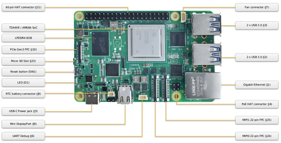
| Connector / Component | Designator | Location |
|---|---|---|
| 40-pin HAT Connector | J11 | Top edge, left |
| Fan Connector | J7 | Top edge, right |
| TDA4VE / AM68A SoC | — | Board center |
| LPDDR4 8 GB | — | Left area |
| PCIe Gen3 FPC | J10 | Left edge, upper |
| Micro SD Slot | J23 | Left edge, center |
| Reset Button | SW1 | Left area, center |
| LED | D1 | Left area, lower |
| USB-C Power | J5 | Bottom edge, far left |
| RTC Battery Connector | J8 | Bottom edge, left |
| Mini DisplayPort | J9 | Bottom edge, left-center |
| UART Debug | J6 | Bottom edge, center |
| MIPI0 22-pin FPC | J24 | Bottom edge, center-right |
| MIPI1 22-pin FPC | J25 | Bottom edge, right |
| PoE HAT Connector | J4 | Bottom area, far right |
| USB 3.0 × 2 | J3 | Right edge, upper stack |
| USB 3.0 × 2 | J2 | Right edge, lower stack |
| Gigabit Ethernet | J1 | Right edge, lower |
System block diagram¶
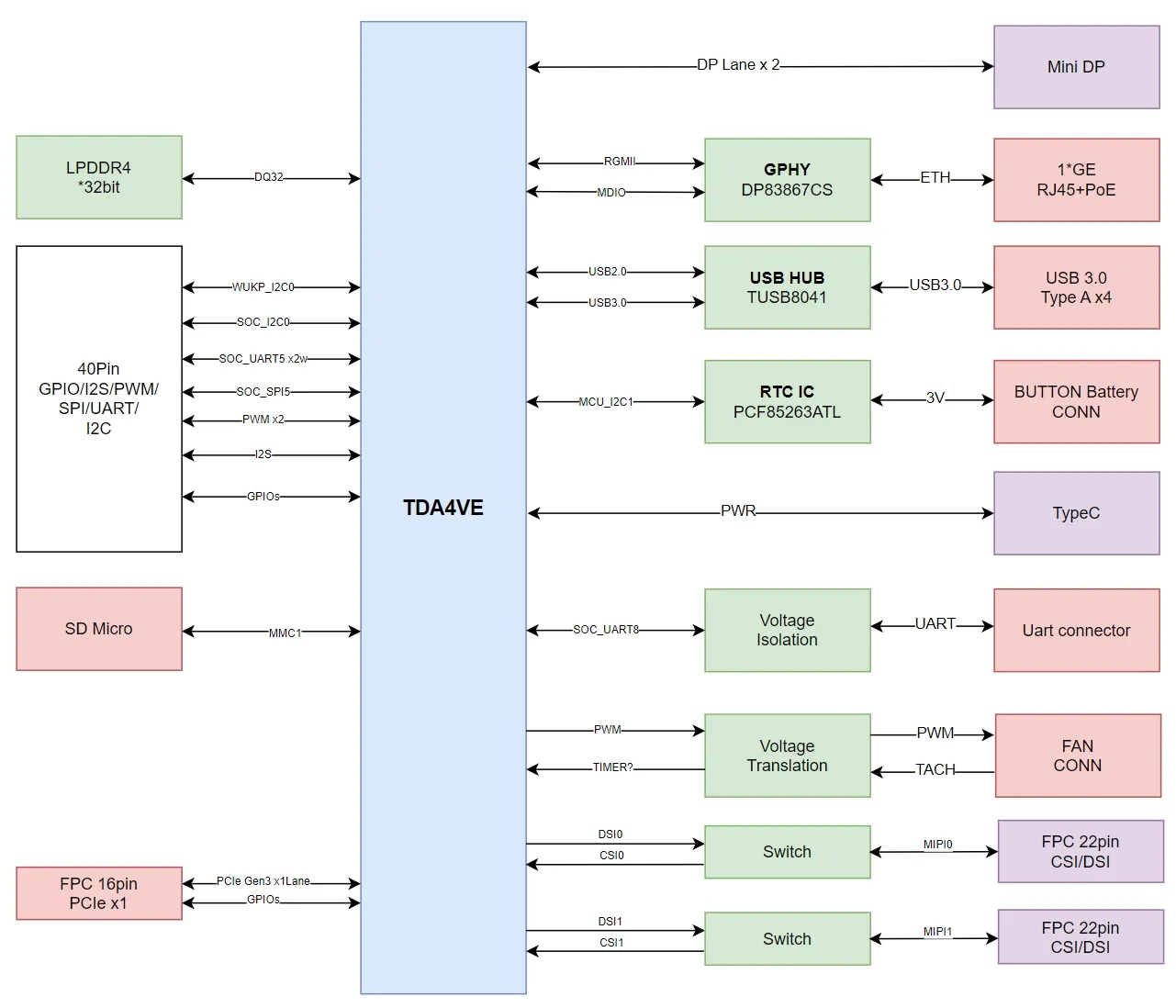
The major subsystems and their interconnects:
| Subsystem | Interface to SoC |
|---|---|
| LPDDR4 8 GB | DQ×32 (DDRSS0) |
| Micro SD card | MMC1 |
| Mini DisplayPort | SERDES0 DP lanes (2-lane DP0) |
| USB 3.0 Hub (TUSB8041) | USB2.0 + SERDES0 USB3.0 SS |
| Gigabit Ethernet (DP83867) | MCU RGMII1 |
| MIPI FPC × 2 | DSI0/CSI0, DSI1/CSI1 (switchable) |
| PCIe Gen3 FPC | SERDES0 PCIe x1 (PCIE1) |
| 40-pin GPIO Header | SOC I2C0, WKUP I2C0, UART5, SPI5, I2S, GPIO |
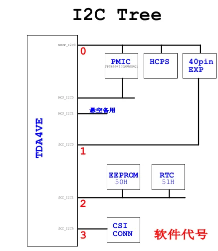
| RTC (PCF85263ATL) | SOC I2C1 (0x51) |
| Board EEPROM (BL24C02F) | SOC I2C1 (0x50) |
| USB-C (power) | USB0 |
| Debug UART (J6) | UART8 |
| Fan | PWM + TACH |
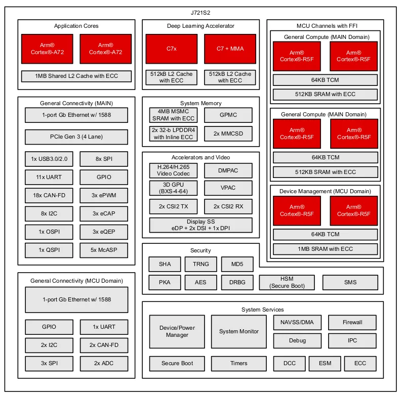
SoC overview¶
Functional block diagram¶
Key parameters¶
| Parameter | Value |
|---|---|
| SoC | TDA4VE / AM68A (J721S2 family) |
| Application CPU | 2× ARM Cortex-A72, up to 2.0 GHz |
| AI Accelerator | MMA (Matrix Multiply Accelerator), 8 TOPS |
| MCU subsystem | Up to 6× ARM Cortex-R5F, up to 1.0 GHz |
| Memory interface | LPDDR4, 32-bit bus |
| Connectivity | 1× USB 3.0 (SERDES), 1× PCIe Gen3 x1 (SERDES), 2× MIPI CSI-2/DSI, 1× DisplayPort (SERDES), RGMII |
| Package | FCBGA |
Refer to the TI J721S2 Technical Reference Manual (SPRUJ28) for complete SoC documentation.
I2C bus tree¶
Power supply¶
USB-C input port¶
Power is supplied exclusively through the USB-C port (J5).
| Parameter | Value |
|---|---|
| Input voltage | 5 V |
| Rated power | 27 W |
| Required adapter current | 5 A minimum |
| Connector | USB Type-C (J5) |
The USB-C port carries board power. Operating long-term at insufficient 5 V current risks resets, storage write failures, or overheating. Connect the USB-C adapter after other peripherals are wired.
Power-on sequence¶
Power sequencing is managed by the PMIC (TPS6594). The reset IC (TPS380833) provides a clean PMIC_ENABLE signal.
Boot configuration¶
| Parameter | Value |
|---|---|
| Primary boot device | Micro SD card (MMC1) |
| Fallback boot device | RGMII (Ethernet) |
| Boot mode pins | Factory-set by resistor strapping |
The boot mode resistors are soldered at the factory and cannot be changed in the field. The primary boot path is SD card; if no valid SD card is detected, the SoC ROM attempts a network boot over RGMII.
Memory¶
LPDDR4¶
| Parameter | Value |
|---|---|
| Capacity | 8 GB |
| Device | Micron MT53E2G32D4DE-046 |
| Bus width | 32-bit (×32) |
| Interface | DDRSS0 on SoC |
| Voltage | DDR_1V1 |
eMMC¶
No eMMC is populated. The MMC0 interface on the SoC is not connected.
Micro SD card¶
The Micro SD slot (J23) is connected to MMC1 on the SoC. It is the primary boot medium and the primary removable non-volatile user storage on the board. For connector electrical details, see Micro SD card slot (J23).
On-board interfaces¶
Power input — USB-C (J5)¶
| Parameter | Value |
|---|---|
| Connector | USB Type-C, 16-pin |
| Voltage | 5 V |
| Current | 5 A (27 W adapter required) |
The USB-C port carries board power (5 V / 27 W). Connect the USB-C power adapter last, after all other peripherals.
Micro SD card slot (J23)¶
| Parameter | Value |
|---|---|
| Connector | MUF-M614 push-push micro SD |
| SoC interface | MMC1 (4-bit) |
| Voltage | 3V3_SD (load-switched) |
The SD slot is the primary user-writable storage on the board and the primary boot medium.
Mini DisplayPort (J9)¶
| Parameter | Value |
|---|---|
| Connector | Mini DisplayPort (20-pin), recessed/sink-board type |
| SoC interface | DP0 via SERDES0 (2-lane) |
| HPD | DP0_HPD (MCASP1_ACLKX, ball AA24) |
| Power | 3V3_DP (load-switched, 500 mA) |
The display output requires a DisplayPort monitor. HDMI monitors are not directly supported.
| J9 signal | SoC signal | Ball |
|---|---|---|
| DP_TX0_P | SERDES0_TX2_P → DP0_TXP0 | AG6 |
| DP_TX0_N | SERDES0_TX2_N → DP0_TXN0 | AG5 |
| DP_TX1_P | SERDES0_TX3_P → DP0_TXP1 | AD8 |
| DP_TX1_N | SERDES0_TX3_N → DP0_TXN1 | AD7 |
| DP_AUX_P | DP0_AUX_P | — |
| DP_AUX_N | DP0_AUX_N | — |
| DP_HPD | DP0_HPD (MCASP1_ACLKX) | AA24 |
USB 3.0 Type-A × 4 (J2, J3)¶
| Parameter | Value |
|---|---|
| Connectors | J2 (lower stack), J3 (upper stack), each 2-port |
| USB hub | TUSB8041 (1× upstream, 4× downstream) |
| SuperSpeed lanes | SERDES0_TX1/RX1 → USB3.0 SS to hub upstream |
| Hi-Speed | USB0 (USB2.0) to hub upstream |
| Port power | 5V_TypeA via TPS2561, up to 3.6 A total across all 4 ports |
| Overcurrent protection | Per-port (PWRCTL, OVERCUR signals) |
The TUSB8041 provides:
- 4× USB 3.0 Gen1 (5 Gbps) downstream ports
- Per-port individual power switching and overcurrent detection
Gigabit Ethernet (J1)¶
| Parameter | Value |
|---|---|
| Connector | RJ45 with integrated magnetics |
| PHY | DP83867 |
| SoC interface | MCU RGMII1 |
| Speed | 10/100/1000 Mbps, auto-negotiation |
| PHY MDIO address | 0x00 |
| LED0 | Link indicator |
| LED1 | Activity indicator |
| PoE | Tap points available (J4, see PoE HAT connector (J4)) |
MIPI camera / display FPC — MIPI0 (J24) and MIPI1 (J25)¶
Both MIPI FPC connectors are 22-pin, 0.5 mm pitch. Each connector can be configured as either a MIPI CSI-2 camera input or a MIPI DSI display output, selected by zero-ohm resistor jumpers controlled by a GPIO (OE/SEL).
| Parameter | J24 (MIPI0) | J25 (MIPI1) |
|---|---|---|
| Connector | 22-pin FPC, 0.5 mm | 22-pin FPC, 0.5 mm |
| CSI-2 source | CSI0 (4 lanes, 2.5 Gbps/lane) | CSI1 (4 lanes, 2.5 Gbps/lane) |
| DSI source | DSI0 (4 lanes) | DSI1 (4 lanes) |
| I2C bus | SOC_I2C5 (Y24/SCL, W23/SDA) | SOC_I2C5 (Y24/SCL, W23/SDA) |
| Power | 3V3_EXP | 3V3_EXP |
| SEL GPIO | WKUP_GPIO0_36 (OE), WKUP_GPIO0_37 (SEL) | WKUP_GPIO0_33 (OE), WKUP_GPIO0_32 (SEL) |
| PWDN GPIO | GPIO0_47 | GPIO0_48 |
FPC pin map (22-pin):
| Pin | Signal | Direction |
|---|---|---|
| 1 | GND | — |
| 2 | DSICSI_D0_N | Differential (data lane 0) |
| 3 | DSICSI_D0_P | Differential (data lane 0) |
| 4 | GND | — |
| 5 | DSICSI_D1_N | Differential (data lane 1) |
| 6 | DSICSI_D1_P | Differential (data lane 1) |
| 7 | GND | — |
| 8 | DSICSI_CLK_N | Differential (clock) |
| 9 | DSICSI_CLK_P | Differential (clock) |
| 10 | GND | — |
| 11 | DSICSI_D2_N | Differential (data lane 2) |
| 12 | DSICSI_D2_P | Differential (data lane 2) |
| 13 | GND | — |
| 14 | DSICSI_D3_N | Differential (data lane 3) |
| 15 | DSICSI_D3_P | Differential (data lane 3) |
| 16 | GND | — |
| 17 | I2C_SCL | 3.3 V open-drain |
| 18 | I2C_SDA | 3.3 V open-drain |
| 19 | GPIO (PWDN / REFCLK) | 3.3 V GPIO |
| 20 | GPIO (RESET) | 3.3 V GPIO |
| 21 | GND | — |
| 22 | 3V3_EXP | Power (3.3 V) |
PCIe Gen3 FPC (J10)¶
| Parameter | Value |
|---|---|
| Connector | 16-pin FPC, 1.0 mm pitch |
| SoC interface | PCIe Gen3 × 1 lane (PCIE1, SERDES0 lane 0) |
| Power | VCC_IN_5V |
| Reference clock | PCIE_REFCLK1_P/N |
Signal summary:
| Pin group | Signals | Notes |
|---|---|---|
| Power | VCC_IN_5V | 5 V supply for PCIe device |
| GND | — | Multiple ground pins |
| TX | PCIE1_TXP0, PCIE1_TXN0 | Gen3, 8 GT/s |
| RX | PCIE1_RXP0, PCIE1_RXN0 | Gen3, 8 GT/s |
| REFCLK | PCIE_REFCLK1_P, PCIE_REFCLK1_N | 250 MHz diff clock |
| PWEN | GPIO0_11 (V23) | PCIe device power enable |
| DET/WAKE | GPIO0_12 (T26) | Device detect / wake |
| RST | GPIO0_19 (V27) | Reset (active low) |
| CLKREQ# | PCIE1_CLKREQN | — |
RTC battery connector (J8)¶
| Parameter | Value |
|---|---|
| Connector | SH1.0, 2-pin (1.0 mm pitch) |
| RTC IC | PCF85263ATL |
| Battery | CR2032 button cell (3 V) |
Pinout:
| Pin | Signal |
|---|---|
| 1 | BAT+ (cell positive) |
| 2 | GND |
The RTC retains time when board power is removed, provided a battery is connected. The PCF85263ATL communicates with the SoC via SOC I2C1 (I2C1_SCL: AC25, I2C1_SDA: AD26), I2C address 0x51.
PoE HAT connector (J4)¶
| Parameter | Value |
|---|---|
| Connector | 2 × 2, 2.54 mm pitch |
| Purpose | Passive tap to Ethernet transformer for PoE expansion board |
J4 provides four centre-tap signals from the RJ45 transformer (TR0–TR3). A separate PoE expansion board is required to extract power from these taps. The RJ45 connector (J1) does not source PoE power by itself.
Fan connector (J7)¶
| Parameter | Value |
|---|---|
| Connector | SH1.0, 4-pin (1.0 mm pitch) |
| Fan voltage | 5 V (VCC_IN_5V) |
| PWM control | PWM1_B (GPIO0_29, R28) via SN74LVC1T45 level translator |
| Tachometer | TIMER_IO1 (AG25) via MOSFET Q7 (NX8008NBKWX) |
Pinout:
| Pin | Signal | Description |
|---|---|---|
| 1 | 5V | Fan power (5 V) |
| 2 | PWM | Fan speed control (PWM) |
| 3 | GND | Ground |
| 4 | TACH | Fan tachometer input |
A 5 V, 4-pin PWM fan is required. The PWM frequency and duty cycle are software-controlled. Connecting the fan is mandatory for thermal management; operating the board without a fan may cause throttling or damage.
40-pin GPIO header (J11)¶
| Parameter | Value |
|---|---|
| Connector | 2 × 20, 2.54 mm pitch, through-hole |
| IO voltage | 3.3 V (VDDSHV domain), not 5 V tolerant |
| Power supply | 3V3_EXP (load-switched, 4 A total shared with MIPI FPCs) |
Note: Three GPIO signals on this header are in the WKUP domain (MCU subsystem). They behave differently from main domain GPIOs with respect to power-down and sleep states.
The header follows the Raspberry Pi 40-pin HAT mechanical footprint and pin numbering. The SoC signal assignments differ from a Raspberry Pi.
40-pin signal map:
Odd-numbered pins (left column), even-numbered pins (right column). Ball numbers shown in parentheses; WKUP-domain pins marked with †.
| Function (odd pin) | Pin | Pin | Function (even pin) | |
|---|---|---|---|---|
| 3.3 V | 1 | 2 | 5.0 V | |
| I2C0_SDA (AE24) | 3 | 4 | 5.0 V | |
| I2C0_SCL (AH25) | 5 | 6 | GND | |
| AUDIO_CLK / GPIO0_30 (Y25) | 7 | 8 | UART5_TXD (W25) | |
| GND | 9 | 10 | UART5_RXD (AC24) | |
| WKUP_GPIO0_60 (E27) † | 11 | 12 | I2S_CLK (AB28) | |
| GPIO0_0 (AG24) | 13 | 14 | GND | |
| WKUP_GPIO0_61 (E28) † | 15 | 16 | GPIO0_27 (V26) | |
| 3.3 V | 17 | 18 | GPIO0_51 (AE27) | |
| SPI5_MOSI (R27) | 19 | 20 | GND | |
| SPI5_MISO (AD27) | 21 | 22 | WKUP_GPIO0_70 (B26) † | |
| SPI5_CLK (T27) | 23 | 24 | SPI5_CS0 (U28) | |
| GND | 25 | 26 | SPI5_CS1 (W28) | |
| WKUP_I2C0_SDA (H27) † | 27 | 28 | WKUP_I2C0_SCL (H24) † | |
| GPIO0_18 (AB27) | 29 | 30 | GND | |
| GPIO0_33 (AA28) | 31 | 32 | PWM / ECAP0 (AB26) | |
| PWM5_B / GPIO0_32 (U26) | 33 | 34 | GND | |
| I2S_FS (U27) | 35 | 36 | GPIO0_10 (AB24) | |
| GPIO0_9 (Y28) | 37 | 38 | I2S_DIN (AC28) | |
| GND | 39 | 40 | I2S_DOUT (Y26) |
Available interfaces summary:
| Interface | Pins | Notes |
|---|---|---|
| I2C (SOC) | 3, 5 | SOC domain I2C0 |
| I2C (WKUP) | 27, 28 | WKUP domain I2C0; shared with PMIC |
| UART | 8, 10 | UART5, full-duplex |
| SPI | 19, 21, 23, 24, 26 | SPI5 (MOSI, MISO, CLK, CS0, CS1) |
| I2S | 12, 35, 38, 40 | MCASP0 (CLK, FS, DIN, DOUT) |
| PWM | 32, 33 | Pin 33 (PWM5_B, U26): available via pwmchip1 ch1; pin 32 (ECAP0, AB26): routed but no kernel DT node |
| GPIO (SOC) | 7, 13, 16, 18, 29, 31, 33, 36, 37 | Main domain GPIO0 |
| GPIO (WKUP) | 11, 15, 22 | MCU subsystem GPIO, remain active in deep sleep |
Indicators, reset, and UART debug¶
LED indicator (D1)¶
D1 is a dual-color LED (KL-3210URSYGC).
| Color | Function | Control GPIO | Ball |
|---|---|---|---|
| Red | Power / boot indicator | WKUP_GPIO0_4 | C23 |
| Green | System status | WKUP_GPIO0_5 | F26 |
Normal operating state: LED turns solid green when Linux has booted and the system is running. During boot, the LED is red. See the Mo 68A User Guide for LED behavior details.
Reset button (SW1)¶
SW1 is a tactile push button that controls PMIC_ENABLE. Pressing SW1 initiates a system reset. The reset IC (TPS380833) provides a debounced, controlled-release reset pulse.
SW1 asserts a full system reset including the SoC, DDR, and all power rails. It is equivalent to a power cycle.
UART debug console (J6)¶
| Parameter | Value |
|---|---|
| Connector | SH1.0, 3-pin (1.0 mm pitch) |
| UART | UART8 (SOC domain) |
| Baud rate | 115200 |
| Frame format | 8N1, no flow control |
| Logic level | 3.3 V |
Pinout:
| Pin | Signal | Ball | Description |
|---|---|---|---|
| 1 | RXD | AF26 | SoC receive (connect to adapter TX) |
| 2 | GND | — | Ground |
| 3 | TXD | AH27 | SoC transmit (connect to adapter RX) |
A 3.3 V USB-to-UART adapter is required. Connect the serial terminal before applying power to capture early boot output.
UART8 is used for Linux system console output and provides a login prompt independent of the display.
On-board IC and peripheral summary¶
USB 3.0 Hub — TUSB8041¶
The TUSB8041 is a USB 3.0 Gen1 (5 Gbps) 4-port hub. It receives USB2.0 (Hi-Speed) and USB3.0 SuperSpeed from the SoC and exposes four USB 3.0 downstream ports on J2 and J3.
- Individual port power switching
- Per-port overcurrent detection
Gigabit Ethernet PHY — DP83867¶
The DP83867 PHY connects the SoC's MCU RGMII1 interface to the RJ45 jack with integrated magnetics. Key configuration:
- PHY address: 0x00
- Auto-negotiation enabled
- LED0: Link, LED1: Activity
RTC — PCF85263ATL¶
The PCF85263ATL real-time clock provides accurate timekeeping with a 32.768 kHz crystal. It is connected to the SOC I2C1 bus.
- I2C bus: SOC_I2C1, address 0x51
- SCL ball: AC25, SDA ball: AD26
- Battery backup via J8 (CR2032)
Board ID EEPROM — BL24C02F¶
An I2C EEPROM stores board identification and manufacturing data.
| Parameter | Value |
|---|---|
| I2C bus | SOC I2C1 (SCL: AC25, SDA: AD26), address 0x50 |
| Write protect | WP pin must be pulled low before writing |
Key component reference¶
| Component | Model | Interface | Notes |
|---|---|---|---|
| SoC | TDA4VE / AM68A (J721S2) | — | 2× A72, 8 TOPS |
| LPDDR4 | Micron MT53E2G32D4DE-046 | DDRSS0 ×32-bit | 8 GB total |
| PMIC | TPS6594 series | WKUP I2C0 | Multi-rail power management |
| CPU power | TPS62871 (HCPS-A) | — | VDD_CPU_AVS, 8 A |
| Core power | TPS62871 × 2 (HCPS-B) | — | VDD_CORE_0V8, 8 A |
| 3.3V DC-DC | TPS62A06 | — | 6 A, main 3.3 V rail |
| USB power switch | TPS2561 | — | 5V_TypeA, 3.6 A |
| USB 3.0 Hub | TUSB8041 | USB3.0 SS + USB2.0 HS | 4-port, Gen1 5 Gbps |
| GbE PHY | DP83867 | MCU RGMII1 | 10/100/1000 Mbps |
| RTC | PCF85263ATL | SOC I2C1 (0x51) | Battery backup |
| Board EEPROM | BL24C02F | SOC I2C1 (0x50) | Board ID |
| Fan PWM translator | SN74LVC1T45 | GPIO/PWM | PWM level translation |
| Fan TACH switch | NX8008NBKWX (Q7) | TIMER_IO1 | TACH signal conditioning |
| Reset IC | TPS380833 | — | PMIC_ENABLE control |
Mechanical dimensions¶
Refer to the PCB layout drawing MO68A_MB_FAB_V1.0.pdf for board outline, hole positions, and component keep-out zones.
The 40-pin HAT connector (J11) follows the Raspberry Pi 40-pin HAT mechanical footprint.
Related documents and resources¶
| Document / resource | Description |
|---|---|
| Mo 68A Quick Start Guide | Initial setup, flashing, first login |
| Mo 68A User Guide | Interface usage, peripheral configuration, system administration |
Revision History¶
| Version | Date | Description |
|---|---|---|
| 1.0 | 2026-04-27 | Initial release. |